(1) Micro Contact Printing Technology (MCP)
The organic polymer solution is used as an ink, applied to the image portion of the silicone rubber plate, and the organic polymer at the raised portion of the plate is transferred to the surface of the printed substrate by the micro contact printing method (Fig. 1). Thanks to the ingenious design of the inventors, the organic polymer is firmly adsorbed on the surface of the substrate to form a concave and convex image of molecular thickness. People call this technology micro-contact printing technology. Here, it should be noted that in the early experiments, an organic high molecular ethanol solution with a mercapto group was used as the ink, and a so-called substrate was a silicon sheet coated with a gold film on the surface. When people transferred a polymer solution containing a thiol group on a silicone rubber plate to a gold film, a self-assembled monomolecular film image was formed. Mizuno and others from the Nanotechnology Research Department of the Japan Institute of Industrial Technology pointed out that in addition to the use of thiol-containing organic polymer solutions as microcontact printing inks, scientists recently discovered chemically active aminosilanes on the surface. It is also a very good ink. The image (mica sheet) printed with this ink was confirmed by atomic energy microscopy (AFM) and a large amount of DNA molecules were adsorbed on the surface of the aminosilane image. It is believed that this is because the positive charges on the aminosilane surface are attracted to the negatively charged DNA molecules.
Micro-contact printing not only has the advantages of being quick and cheap, but also does not require the harsh conditions of the clean room, and does not even require an absolutely flat surface. Micro-contact printing is also suitable for a variety of different surfaces, with flexible and versatile operating methods. The disadvantage of this method is that at the submicron scale, the diffusion of mercaptan molecules during printing will affect the contrast and widen the printed image. By optimizing the ink immersion method and the immersion time, especially controlling the amount and distribution of ink on the dies, the diffusion effect can be reduced.
(2) Capillary micro modeling (MIMIC)
That is, a printing plate having a nano concave-convex image is placed on the surface of the substrate. At this time, the irregularities of the plate image and the surface of the substrate form a very fine gap (capillary), and then the liquid polymer is dropped on the silicone rubber plate. Due to capillary action, the liquid polymer enters these gaps on its own. If we solidify the polymer in the gap and separate the two, a fine nano-convex image can be obtained. This technology can be widely used in the manufacture of optical components and the like.
(3) Micro-transfer modeling (mTM)
That is, the prepolymer is used as an ink and applied to the depressions of the silicone rubber plate. The prepolymer is transferred to the surface of the substrate by a transfer method, and then heated and cured to form a nano concave-convex image. We call this printing method micro-transfer modeling.
(4) Near-field phase shift printing (PSL)
After applying the photoresist coating on the substrate, the silicone rubber mold is used to transfer the image on the resist coating and use it as a contact exposure mask, such as exposure to ultraviolet light. Since the concave and convex pattern transferred by the silicone rubber mold induces a phase shift, it is possible to form an image. However, the premise is that the size of the image asperities is smaller than the wavelength of the ultraviolet light, and the effect of near-field light can make image transfer a reality. Recently, it has been reported that nanometer images can be formed on a spherical surface by using this technique.
In addition, there are nanochemical lithography. It is one of the newest types of self-assembly technology for nanomaterials. In the scientist's demonstration, this process can effectively form a very stable nanoparticle cycle array without prior lithography (eg, atomic force microscope dip printing, laser lithography, electron beam lithography, rolling) Many limitations and limitations in printing, etc.). Nano-chemical lithography involves the production of nano-sized periodic template technology that requires absolute control of size, size, spatial distribution, and functionality. Nanochemical lithography is a combination of multiple technologies in which the alignment of particles is controlled by reflecting the difference in activity, and the reactivity is determined by the type of chemical treatment the particles and their surfaces are exposed to.
Scientists use gamma-ray yttrium aluminum (YAG) nanoparticles that are polymerized on silicon chips to synthesize additive particles and crystallize them to determine their shape and composition. Before the nanoparticles were polymerized on a silicon chip, scientists used an etching technique based on the "atomic stepping" phenomenon to engrave the template in advance on the silicon chip. Because of the high order of atoms that naturally exist on the silicon chip's surface, scientists can move these atoms through processing to create the desired template. A thin layer of nitride formed by a chemical reaction (between silicon, nitrogen, and oxygen) is correspondingly formed on the boundaries of the atomic steps so that the template is pre-engraved on the chip. In order to align the particles along the template on the chip, the scientists placed the sample in an ultra-high vacuum chamber and anneal for several hours. After processing at 500 - 850 degrees Celsius, not only nanoparticles based on the model's precise alignment were obtained, but also another advantage was obtained. After using this technique to measure quenching, the nanomaterial arrangement can also show its strength. In general, many nanoparticles are subjected to photobleaching. This damage is caused by exposure to high-intensity light. On the other hand, these particles retain their light in the extended illumination of the fluorescence imaging measurement technology of scientists. The initial state.
In a word, nano-image printing is not a printing technique with traditional meaning. It is a newly emerged so-called soft printing technology. This technology breaks through the limits of today's printing accuracy (micron level) and pushes the printing to the nano-processing scale. As a result, it has become one of the important means for the manufacture of nanostructures, nanodevices, and even nanomachines. Nano-imaging technology is currently considered to be the closest to practical manufacturing technology. It indicates that profound changes are taking place in the field of fine processing. The manufacture of ultra-fine images with nanostructures will come out of scientists' laboratories and move quickly toward practicality. Japan currently has nanometer printing devices on the market. However, in order to form a good structure, it is necessary to develop related technologies that use nano-templates and resin materials as precursors. This research is currently underway throughout the world. The application of nano-image printing technology is mainly focused on electronics and microelectronics, but it has also started to involve areas such as marginal energy. With the continuous deepening of the research on soft printing technology represented by nano-image printing technology, it will certainly promote a far-reaching revolution in electronics, microelectronics, printing and other related technologies.
A Brief Analysis of Nanometer Image Printing Technology
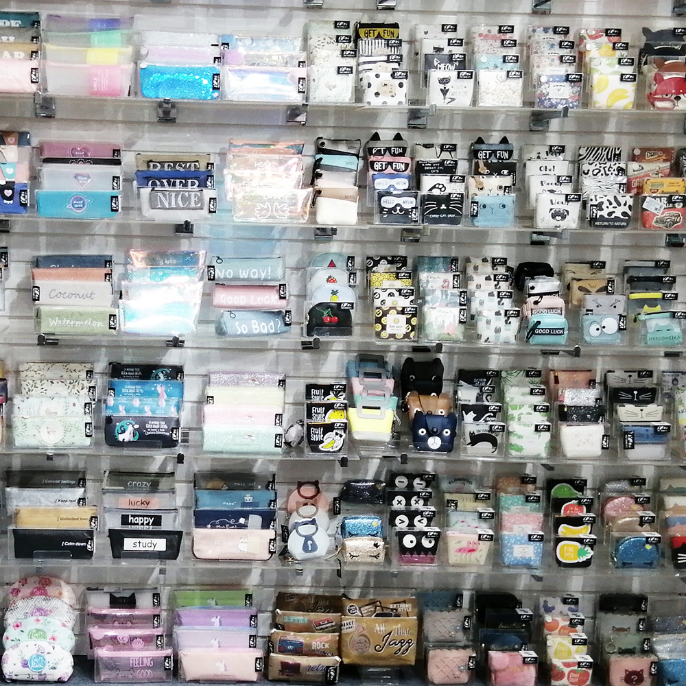
The Laser TPU Coin Purse is more convenient to carry, comfortable to feel, and easy to clean, so that the most things can be packed in the smallest space. Digital printing, silk-screen printing, and other printing methods and accessories combination for relevant design, is the combination of practicality and aesthetic culture.


Laser Tpu Coin Purse,Wallet With Coin Pocket,Mens Coin Purse,Leather Coin Pouch
Jilin Y.F. Import & Export Co.,Ltd , https://www.jlpencilcase.com