Lasers Carve MM-Wave Circuits
A laser-based circuit milling system capable of working with a wide range of circuit materials provides the feature resolution needed o reliable fabricate circuits for millimeter-wave applications.

Challenge:
Millimeter-wave frequencies represent largely unchartedbandwidth
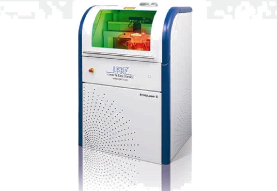
Hopingto explore the region further, Germany's Fraunhofer Institute for Applied SolidState Physics, named after Joseph von Fraunhofer who investigated theproperties of visible light as early as 1820, has enlisted the aid of aProtoLaser S system from laser-machining specialist LPKF Laser & Electronics for rapid fabrication of prototype circuits on a wide range of printed-circuit -board (PCB) materials.
The Fraunhofer Institute is involved in not onlyengi-neering new solutions for millimeter -wave devices and components, but inenabling their use in practical ap-plications. For example, high frequencyradiometers can be used to continuously measure the temperature and humidity ofthe atmosphere using a ground -based system. Millimeter-wave circuits are alsoused in radar, in airport body scanners, in industrial metrology, safetyengineering, astronomy, and in environmental surveys.
Inorder to explore the commercial deployment of its millimeter -wavedevelopments, the Fraunhofer Institute needed the means of fabricatingfine-featured circuits from a variety of different PCB substrate materials. TheProtoLaser S system from LPKF uses high-energy pulsed laser beams toselectively ablate the conductive layer ( usually copper) of a PCB laminate toform the thin transmission lines and circuit structures needed in support ofmillimeter-wave frequencies.
Solution:
The LPKF ProtoLaser S
A compact, laboratory-qualified laser system designed specifically for prototyping as well as on-demand small batch production of PCBs. It is equipped with casters for mobility and requires only compressedair, a vac-uum, and a standard 110-VAC power outlet. Using a patented process, the laser can structure circuitry with great precision on most circuitsubstrates. The laser beam circumscribes the contours of circuit artwork onfully clad PCB material, thus producing the wiring structure.
Thelaser system can process circuit layouts as large as 229 x 305 mm with astructuring speed of about 1 in. 2 per minute (6 cm2 per minute). It works with flexi-bleand rigid substrate materials, including copper-coated FR-4, polytetrafluoroethylene (PTFE), and ceramic substrates. The contact-freeprocess results in handling sensitive materials without damage, resulting inhigh yields. The best precision is when using ce-ramic materials. On ceramicmaterials, the conductive layer is vaporized, allowing for conductor trackswith a width of only 50 μm (0.002 in.) and spacing as small as 25 μm (0.001in.). Process parameters can be stored in memory for future research or small production runs. The ProtoLaser incorporates an internal forced-air coolingsystem for long-term reliability . The system measures 34.5 x 56.3 x 29.5 in. (875 x 1430 x 750 mm) and weighs 573 lbs. (260 kg).
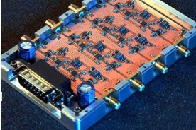
The Fraunhofer Institute has used the ProtoLaser S system to fabricate circuits for millimeter-wave applica-tions, including a four -channel intermediate frequency (IF) amplifier for a 94-GHz radar system

High-frequency circuits such as this four -channel IFamplifier for 94-GHz radar modules are produced quickly
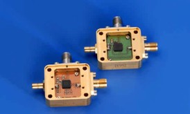
The system has also been used to produce a 15-GHz voltage controlled-oscillator (VCO) circuit for a multi-plexer that generates signals in the 90-GHz range

This 15-GHz VCO was optimized using the ProtoLaser Ssystem to fabricate different circuits, including a test board (left) and finished circuit (right).
Results: Productivity Gain
Engineer Michael Kuri, one of the specialists at the Fraunhofer Institute on combining RF semiconductors with circuit carrier systems, confirms the productivity gain when using the ProtoLaser S system:
"Our measurements demonstrate that boards pro-duced with the LPKF ProtoLaser S are in no way inferior to prototypes produced externally. How-ever, in-house prototyping facilitates several itera-tion cycles per day and production on demand."
Having the ProtoLaser S system on site at the Fraun-hofer Institute allows its engineers to react quickly when modifications to a design are needed. For example, Kuri mentions the development of a slot antenna for an innovative radar system. The antenna required virtually radii- free cut-outs in order to achieve the r a-diation properties needed for the radar system. The production time to produce the antenna with previous machining services and methods was three days or more; with the ProtoLaser S system, this was reduced to two minutes
Fraunhofer is Europe's largest application-oriented research organization. Research is geared entirely to people's needs: healthy, security, communica-tion, energy and the environment.
LPKF Laser & Electronics AG manufactures ma-chines and laser systems used in electronics fabri-cation, the automotive sector, and the production of solar cells. Around 20 percent of the workforce is engaged in research and development.
Toilet Paper Roll,Toilet Tissue Virgin Wood Pulp,Toilet Roll Paper,Toilet Tissue Paper Roll
Baoda Paper Enterprise Co., Ltd. , https://www.baodatissue.com